Did you know that the world’s first computers filled entire rooms? Now we can carry even more computing power than those early machines in the palm of our hands, thanks to advancements in nano- and transistor technology. Transistors are the components in a computer that control the flow of electricity and therefore allow the computer to process information. In the past, each transistor was the size of a light bulb and had to hold minimum temperatures of ~1000˚F.1 Now, transistors are made of a semiconducting material that allows transistors to be down-sized to the nanoscale. But getting down to the nanoscale can actually make it hard for transistors to do their job.
The most popular semiconducting material for making computer transistors is silicon (hence the name Silicon Valley). Alone, silicon cannot control the movement of electrons, so an impurity must be added in a process called doping, typically with boron, phosphorus, selenium or germanium.2 Once the silicon is doped, the movement of electrons can either be turned on (allowing the flow of electrons), or off (stopping the flow of electrons), using a voltage. This on and off status translates perfectly to the binary language of computers, which is composed of different combinations of ones and zeros that tell the device what to do. Multiple transistors are combined into what is called an integrated circuit (IC). The number of transistors that can fit in an IC is called a transistor count. The more transistors in a device, the more combinations of binary codes it can process. This means the device will be faster and can execute more tasks. The fact that you can check your email, play a game, and listen to music on your phone all at the same time is largely a result of nanotechnology helping to shrink transistors!

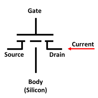
The most commonly used transistor is called the Metal-Oxide-Semiconductor Field-Effect Transistor (MOSFET), which was formulated in the 1960s, shortly after the invention of the IC.3,4 This transistor is composed of 5 main parts: the gate, channel source, drain, and body. The body is typically made of semiconductor materials like the doped silicon I described, to facilitate the flow of electrons. The electrons flow from the source to the drain through the channel, which is controlled by the gate. By applying a voltage, we can cause the gate to block the channel, turning the flow of electrons on and off. 5
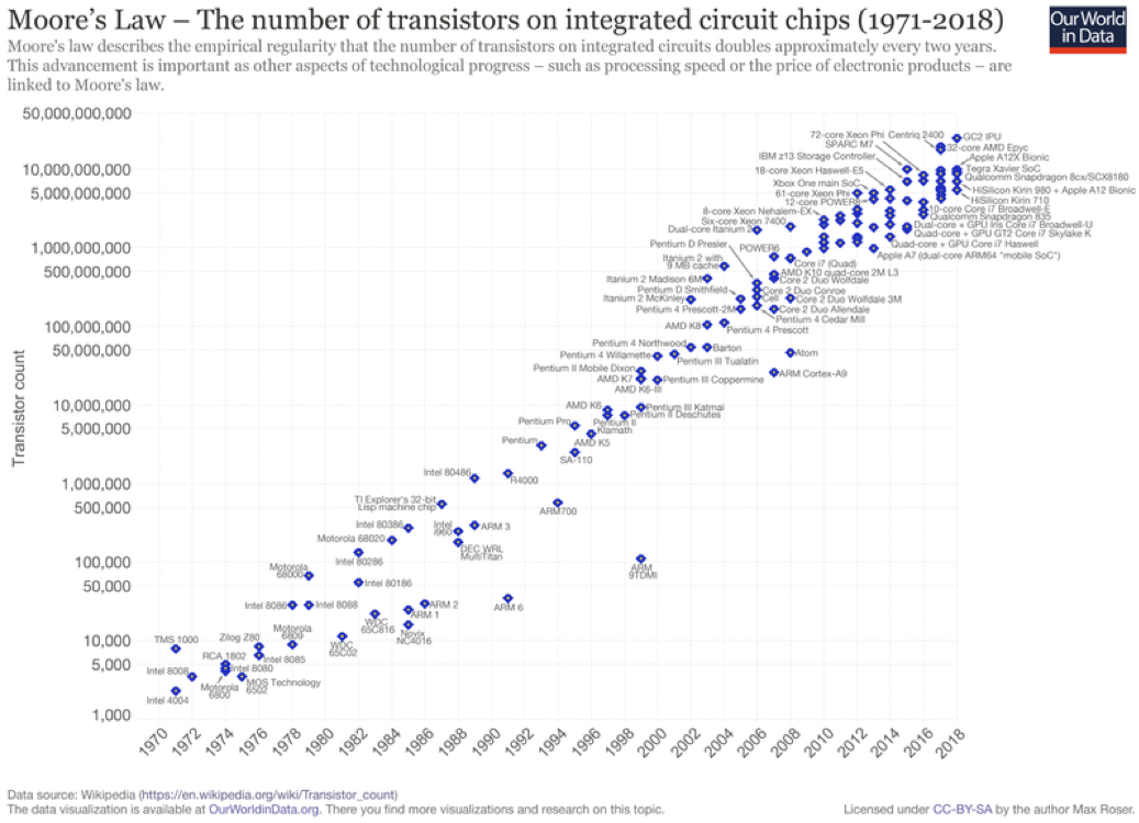
The transistor channel was originally about 10 micrometers in size (10,000 nm, roughly half the width of a human hair.6) Through advancements in physics and semiconductor technology, the size of the channel has decreased to the tens of nanometers, to the point that there can be 100 million transistors per square millimeter.7 In fact, transistor count has increased in a predicted trend known as Moore’s Law. The CEO of Intel, Gordon Moore, predicted in a 1965 paper8 that the transistor count would double every two years.
However, as transistors reach the nanoscale, we enter into the world of quantum mechanics. At such small sizes, the classical behaviors of matter and energy are different. The quantum effect that alters the performance of nanotransistors is called electron tunneling. Electron tunneling is like teleportation: when materials are really thin (less than a nanometer), the electrons can move right through them. In the context of our transistor, this means the gate cannot prevent the flow of electrons through the channel. If the transistor’s control of on and off no longer exists, it cannot speak binary, and your processor is useless!
But in addition to causing problems with silicon transistors, nano-scale effects have the potential to open up lots of possibilities for new transistor technology. For example, some researchers are exploring ways to use 2D materials like molybdenum disulfide to improve the transistor channel. Others are changing the material used for the gate from silicon dioxide to hafnium dioxide nanorods. (To read lots more detail about these new innovations, check out Hayley Bennett’s article, “The search for the new silicon.” )
Transistors have come a long way since their early days, allowing computers to shrink from the size of cars to the size of a wrist watch. With the help of nanotechnology, Moore’s Law may continue far into the future.

EDUCATIONAL RESOURCES
- PBS: Transistorized! teacher’s guide
- STEMRobotics: Moore’s Law instruction guide
REFERENCES
- Lamptech. The First MA Lamp. 2003.
- Laube, P. Fundamentals: Doping: n- and p-semiconductors. Semiconductor Technology from A to Z (website, n.d.)
- Datta, S. Lessons from Nanoelectronics: A new approach to transport theory, Vol.1 in Lessons from Nanoscience: A Lecture Notes Series, World Scientific Publishing Company, Singapore, 2012. DOI: 10.1142/8029
- Lundstrom, M. nanoHUB-U: Essentials of MOSFETs. Online course: https://nanohub.org/courses/mos, 2019.
- Cress, C. & Datta, S. Nanoscale Transistors – Just Around the Gate? Science, 2013 (6142), 140-141. DOI: 10.1126/science.1240452
- Wolfram Alpha
- Bennett, H. The search for the new silicon. Chemistry World, January 2018.
- Moore, G.E. Cramming more components onto integrated circuits, 1965. Electronics, 38(8) 114-117. reprint DOI: 10.1109/N-SSC.2006.4785860

