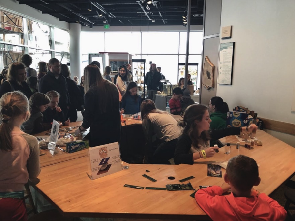
It’s hard to turn down an opportunity to share how cool nanoscience is with the public, and especially with children. Back in February, a group of CSN affiliated women hosted an activity at the Science Museum of Minnesota for their Women in Science and Engineering Day. As members of the Center for Sustainable Nanotechnology, we wanted to share a demonstration that merged both nanoscience and technology. We found the perfect thing: an activity that teaches about photolithography with s’mores!

We called our activity “Life is S’more Fun with Nanoscience,” and used it to introduce children (and frequently parents) to the concept of “nano” and the process of lithography. The activity culminated in a delicious and beautiful dessert!
Defining Nano
Before we could explain photolithography, we thought it was important to teach the definition of nano. Depending on the age of the child, this explanation involved either a lesson in the metric system, an analogy to how many nanoparticles you could fit across the average human hair (around 1,000 assuming a 100 nm particle), or just saying “teeny teeny tiny.” Regardless, we were able to show museum visitors two actual examples of nanoparticles: gold and iron oxide.

Children and adults alike were astounded at the color changing properties of gold as the particles approached the nanosize (you can check out a blog post that briefly discusses the color of gold nanoparticles here), as well as the beautiful designs of the ferrofluid (nanoscale iron oxide – you can read about the applications of magnetic nanoparticles to treat cancer here). To really appreciate how different ferrofluid is from bulk-scale iron filings, it helps to see it moving. With these simple demonstrations we could visually communicate how being small can change the properties of things we might be very familiar with:
Nano in technology
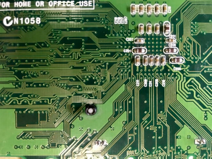
After our visitors saw some of the special characteristics that come with being nano-sized, we showed them the intricate circuitry in RAM cards from computers as an example of how nano is applied to technology. We explained that some of the circuitry in modern devices is even smaller than the pathways that are visible on the RAM cards, which enables technology to keep on getting faster and smaller! We wanted to share how something so small could be made. Both RAM cards and nano-scale circuitry are printed using a technique called lithography.1 Lithography comes from the Greek for “stone writing.” It describes a process invented in 1796 for etching a pattern onto a stone surface. First a repelling product such as oil or fat is used to draw a pattern on a fine grain limestone. Then the limestone is washed with acid, which will etch the stone that is not protected, thus revealing a negative image of the original drawing.

This process has also expanded to design of electronic components such as circuit boards, a method called photolithography (“light stone writing”). When applied on the nanoscale, this is, of course, called nanolithography.
Photolithography enables the fabrication of very precise and detailed design for the complex surfaces of electronics, which is important as more and more nanotechnology is being developed. Instead of acid to etch the lithography surface, it uses ultra-violet light to develop the first design. The first step in photolithography is to prepare the substrate (the main material you want to etch the pattern on) by cleaning and oxidizing the surface and then coating it with a light sensitive chemical called a photoresist. Photoresists comes in two types: positive photoresist which becomes soluble and can be washed away after it is exposed to light; or negative photoresist which becomes insoluble when exposed to light, so it stays in place when everything around it is washed away.
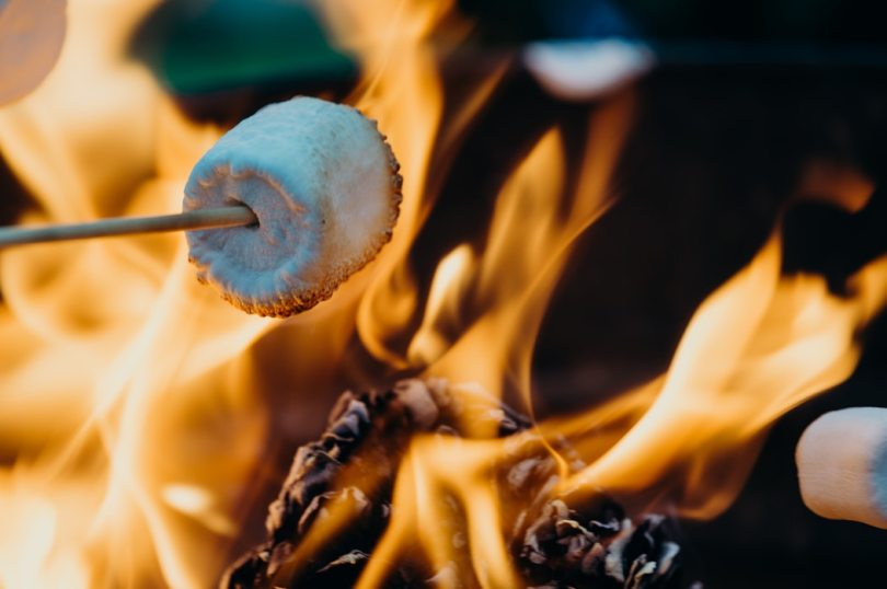
After you add the photoresist coating, you then add a layer called a mask, which is used to block UV light in a certain pattern. Depending on your type of photoresist, either the positive or negative pattern from the mask will appear after the light-exposed photoresist is washed away. Then a chemical etching process occurs to create the pattern in the substrate and finally the resist is washed away. Although we had a diagram to show the process, the tastiest way to learn about lithography is definitely with marshmallows.

S’Mores!
In the s’more activity, we use aluminum foil (the mask) to protect the marshmallow (the photoresist) from a heat gun (UV light).

Before we brought this activity to the museum, we HAD to test it out first (yum!). We found that we needed at least 6 layers of heavy-duty aluminum foil to act as a sufficient photoresist, or else the whole marshmallow would start to burn. We also found that it helped to leave the marshmallows open to the air for a couple days — allowing the exteriors to dry out encouraged them to brown more quickly. For the same reason we chose to use a heat gun instead of a hair dryer. Hair dryers don’t get hot enough to cause browning, but will make your marshmallow nice and soft. Since we wanted to reach as many kids as possible, we provided pre-cut designs (squares, smiles, stars, etc.) for the youngest learners and let older kids cut their own designs.

We organized the activity so that groups of kids would walk around the table, first learning from a volunteer about the size of nano, then to another volunteer to learn about the process of lithography and see the circuitry in electronics, and finally to create and assemble their delicious s’more designs with another three volunteers. In just a few hours, we had made 300 s’mores!
If we took the s’more-lithography analogy all the way through, the next step would be to remove part of the marshmallow: either the toasted part (positive photoresist) or the untoasted part (negative photoresist). The remaining marshmallow would then be stuck to the substrate (graham cracker and chocolate). And every copy would be very similar, because we would use the same mask over and over. This is one reason photolithography is so useful in nanotechnology: it is relatively easy to make many copies of the same design because of the way the mask, photoresist, and substrate are set up and exposed to UV light. You can read a lot more detail about nanolithography in this blog post.
Overall, this activity is a great way to learn about lithography, whether you are a scientist doing a museum demonstration, or just someone with some aluminum foil, marshmallows, and a camp fire!
REFERENCE
- Mack, Chris. Semiconductor Lithography (Photolithography) – The Basic Process. Lithography (website 2006-2019)

