Last July, IBM announced that it had developed a new computer chip that could boost computer speeds by 50%.1 The company achieved this performance boost by building their chip with transistors a mere 7 nanometers in diameter. To put this incredible feat of engineering into perspective, the building blocks of these new chips are smaller than the virus that may cause you to get a cold this winter!
July was a bit slower for me than it was for the folks at IBM, so one day I decided to go to the beach. Due to my hasty and incomplete application of sunscreen earlier in the day, I developed a sunburn which left a strange pattern on my skin and a small blister on my shoulder. You might be wondering what IBM’s hard work and my sunny day at the beach have in common. It may seem far-fetched, but these events are actually related: both IBM’s new speed secret and my beach mishap involve ultraviolet (UV) light.

Before we delve into this tale of blisters and transistors, let’s take a moment to recognize some of the giants on whose shoulders IBM stands with its most recent achievement. The first electronic computers used vacuum tubes as the building blocks of their computational power, but these tubes added tremendous bulk to their hardware and required a huge amount of power. Earlier vacuum tube computers required entire rooms dedicated to their use (check out the size of the computer in Figure 2!).

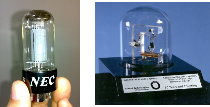
In 1954, Bell Labs introduced one of the first computers that used transistors — small semiconductors — instead of vacuum tubes (shown in figure 3).
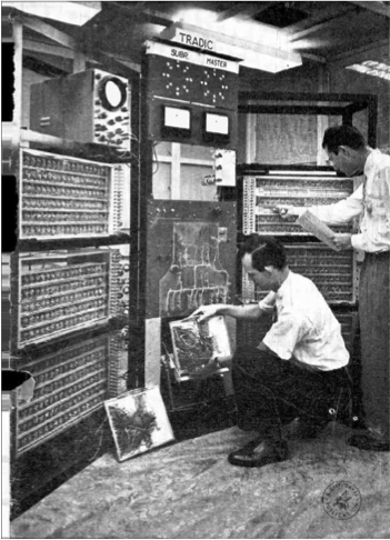
This new transistor-based computer was creatively named the Transistor Digital Computer (TRADIC—see Figure 4). The advent of the transistor allowed for much smaller, more robust, and more energy-efficient computers; the TRADIC was so small, reliable, and low-power that it could even be installed on military airplanes.
Transistor technology continued to advance at an astonishing rate—so rapidly, in fact, that in 1975 Intel co-founder Gordon Moore made a bold prediction. Moore predicted that the number of transistors that could be used on a single computer chip—and thus the processing power of the computer itself—would double every two years. This prediction, now known as Moore’s Law (see Figure 5), has been accurate for the last 40 years due to continuous technological advances in chemistry, physics, and electrical engineering. The most recent of these advances, which will bring us back to the idea of UV light, is Extreme UV Lithography.

In order to understand Extreme UV Lithography, it helps to remember how sunburns happen. Without sunscreen (or a t-shirt, like our trendsetting stickperson in Figure 6 below) to block UV light from penetrating our skin, the UV radiation causes damage in the form of redness and blistering based on levels of exposure. Photolithography is an application of the same effect to make transistors for computers. Light, most often UV light, is shone on a surface and induces a chemical change. Just as a shirt can protect portions of your skin from UV light damage, an opaque material called a mask can protect portions of the transistor surface from the changes caused by the UV light.

The precision of this method to create small and complex shapes on surfaces is limited by the wavelength of the light used in the reaction. You can’t mask shapes that are smaller than about a quarter of the wavelength of light hitting the surface, at best. Creating nano-structures (like the new transistors developed by IBM) requires very precise masking, which in turn requires very short wavelengths of light. Conventional UV lithography can create features as small as 45 nanometers; to create features smaller than that, UV lithography must be pushed to the extreme.
Extreme UV (EUV) lithography uses light in the so-called “extreme ultraviolet” range: while visible light wavelengths are in the range from about 400 to 700 nanometers, extreme UV wavelengths range from 10-124 nanometers, on the edge of the X-ray range of the spectrum (Figure 7). Working with this light is a challenge, because special lasers, mirrors, and high-quality vacuums must be used, and EUV light takes a lot of energy to produce.

July’s announcement demonstrated that many of these challenges are well on their way to being overcome. Scientists and engineers have been able to use EUV lithography to create patterns and features less than 10 nanometers in diameter, enabling IBM’s development and the latest contribution to Moore’s law. Meanwhile, my skin has healed, and while UV exposure hasn’t made me any faster than I was before, I do have a newfound appreciation for EUV lithography and its contribution to the increasingly amazing miracle of modern computing.
EDUCATOR RESOURCES
- Journal of Chemical Education activity by Haynes et al.: Nanopatterning with Lithography (requires subscription access)
- Johns Hopkins Center for Education Resources video by Dave Filipiak: Intro to Micro/Nanotechnology, Micro/Nanodevices and Micro/Nanofabrication Techniques (lithography explanation begins at 5:30)
- IBM (2015) IBM Research Alliance Produces Industry’s First 7nm Node Test Chips [press release]. Retrieved from http://www-03.ibm.com/press/us/en/pressrelease/47301.wss

