Human beings have been trying to figure out the elementary composition of the universe since the era of ancient Greece. Democritus, an ancient Greek philosopher, created atomic theory. In the atomic theory, everything is composed of “atoms” (from the Greek meaning “can’t be cut”) and these atoms are physically indivisible.1 The ancient Greeks speculated on the shapes and connectivity of atoms. For example, they suggested that iron atoms were solid and strong and that water atoms were smooth and slippery.2 Although these ideas are missing key points from our understanding today, they were an important step in philosophy and inspired scientists to develop the modern atomic theory.
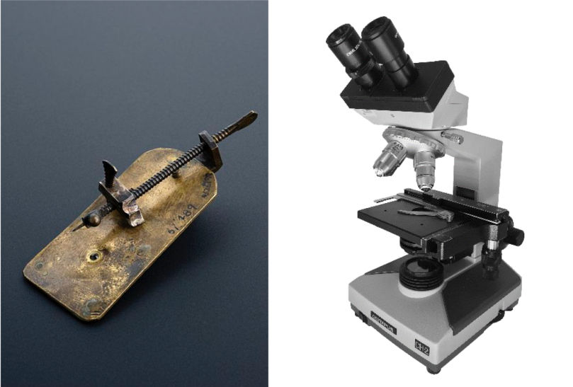
The ability to manipulate light using glass lenses changed humanity’s investigative abilities. In fact, the understanding of the microcosm did not move forward until the invention of the microscope. In the 17th century, Anton van Leeuwenhoek of Holland started to use a set of magnifying glasses to observe the micro-world.3 Since living cells are in the range of 10-100 microns in size and visible light has wavelengths around 400-700 nm (1,000 times smaller) Leeuwenhoek was able to observe the basic unit of all organisms for the first time.
Despite the ability to manipulate visible light, our understanding of the microscopic world remained limited. It took three hundred years after the invention of the microscope before scientists were convinced by a new atomic theory that matter is composed of different elementary atoms. In fact, the modern Periodic Table itself is 150 years old this year! This modern view of atoms supported that a chemical reaction is a process where atoms are combined, separated or rearranged.4 However, there was no way to observe the arrangement of atoms directly even with the best microscope at that time because the wavelength of visible light is way longer than the diameter of a single atom. Remember: the wavelength of visible light is between 400-700 nm. The diameter of an atom is only about 0.1 to 0.5 nm,5 which means looking at an atom with a light microscope is like trying to measure a sesame seed with a yard stick.

Fortunately, scientists started to manipulate and visualize X-rays at that time. An X-ray has a wavelength that is much shorter than visible light (0.001 – 0.1nm) but similar to the size of atoms. The structures of a crystal were first successfully determined by shining X-rays onto it.6

X-rays undergo diffraction when they come across the atomic arrays of crystal structures. Diffraction is adding up or subtracting waves which form unique patterns, just like the circular waves you sometimes see at a coastal quarry. By applying X-ray diffraction (XRD), we are able to analyze crystal structures. This ability is the foundation of solid state physics, which is also one of the foundations of the modern semi-conductor industry. People are still using this technique to probe the arrangement of atoms in crystals, proteins and even viruses.

Although this was a huge step, shooting X-rays is not the end of the story. The wavelength of X-rays is still not small enough to distinguish every single detail in the micro- (or nano-) world. Besides that, it is hard to focus X-rays on a tiny spot. Compared with visible light and X-rays, electrons have an even shorter wavelength! Although they are not part of the Electromagnetic Spectrum, they can still be used for microscopy. Plus, they can be manipulated by a magnetic field. Those features make electrons an ideal candidate to probe into the nano-world.
The first transmission electron microscope (TEM) was made by German scientist in 1933.7 The structure of TEM has not changed much since then. But the resolution has improved dramatically; now we are able to visualize the shape of an atom.8 Recently, the electron even took a selfie: the shape of electrons were successfully projected onto screen by electrons themselves!9

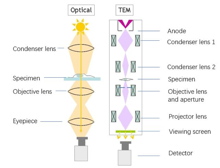
In a modern TEM, the essential components are the electron gun, electron lenses, apertures, sample holder, viewing screen, and camera.7 In the electron gun, high temperature or an electron field excite electrons from a metal or a crystal. Electron lenses are like glass lenses in a light microscope, in that they help to focus the rays to a point. Apertures (small holes) help to control the range of electrons going into the electron lenses. In order to see the image the electrons project, we have to convert electrons to light, which we do using of a process called cathodoluminescence. The viewing screen is often made of modified zinc selenide, which gives off light at 550 nm (green light).7
You may wonder what we can see using a TEM. We can see things as small as a nanometer in size and the nano-world is sometimes beautiful and fantastic! Some great examples come from entries in JEOL USA’s SEM/TEM/EMPA Image Contest. The first sample TEM image below looks like a drawing of rose, while it is actually a nerve fiber gone awry among other brain cells. The other one is quite like a cute walking rabbit. Guess what it actually is? It is lithium metal oxide nanoparticle (often used as battery cathode). This image is taken under cryo-TEM which utilize liquid nitrogen to freeze samples. (I’m not sure where the pink color comes from, but the contest rules rules just require “careful and competent use of image processing and colorization” so it could have been added to emphasize the rabbit-ear effect for this artwork.)

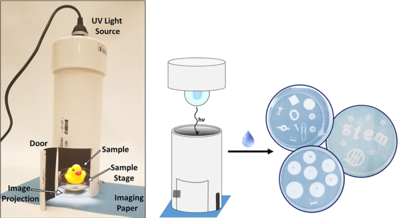
TEM is a fantastic tool to see things as small as nanometer size, but that ability comes at a high cost to construct and operate. To make electron microscopy concepts more available to students, Natalie Hudson-Smith (a fellow graduate student in the Center for Sustainable Nanotechnology and frequent contributor to the blog) designed a model TEM that can be built for less than $50. In this model TEM, a UV bulb is used to represent the electron beam and a UV sensitive cyanotyping paper is used for imaging. You can read more about how we’ve used the model for outreach in this blog post, and Natalie and colleagues published a paper about it in the Journal of Chemical Education.10 That paper showed that through participating in hands-on activities with this model TEM, students got a sense of how to determine the size of an object imaged and understand the function of a scale bar. They also understood that TEMs produce 2D images from 3D objects, learned about spatial reasoning by changing sample “tilt,” and gained a lot of confidence in their understanding of the science behind TEM.10
In many senses, our understanding of the microcosm is determined by how fine-tuned a probe we are using. It has been almost a hundred years since the invention of TEM and this technique is hugely successful in showing the micro- and nano-world. Nowadays, when opening scientific journals, most of the nano-technology related papers mention TEM techniques. However, there are still lots of open questions to be solved in the future: How much more we can do with state-of-art TEM? Would there be a better probe particle other than electrons? Maybe, future scientists will find out and probe even deeper.
REFERENCES
- Bertrand Russel. History of Western Philosophy. London; New York: Routledge, 2004, 76.
- Ernst Cassirer. An Essay on Man: An Introduction to a Philosophy of Human Culture. New Haven: Yale University Press, 1944, 214.
- Ford, Brian J., First Steps in Experimental Microscopy, Leeuwenhoek as Practical Scientist, The Microscope, 1995, 43(2), 47-57.
- Agnew, M. et al. Indivisible – The Atomic Theory. LibreText: Chemistry (website), 2019.
- Friedrich et al. Interferenzerscheinungen bei Röntgenstrahlen. Annalen der physic, 1913, 971-988. doi: 10.1002/andp.19133461004
- Elert, G. (ed). Diameter of an Atom. The Physics Factbook (website).
- Williams, D. et al. Transmission Electron Microscopy. Springer, Boston, MA. 1996, 3-116.
- Greg et al. Atomic Scale Imaging of Competing Polar States in a Ruddlesden–Popper Layered Oxide. Nature Communications, 2016, 7, 12572. doi: 10.1038/ncomms12572
- Zylstra et al. Using Inertial Fusion Implosions to Measure the T+ 3He Fusion Cross Section at Nucleosynthesis-Relevant Energies. Physical Review Letters, 2016, 117(3) 035002. doi: 10.1103/PhysRevLett.117.035002
- Hudson-Smith et al. A Macroscale Model for Hands-On Activities Demonstrating Transmission Electron Microscopy. Journal of Chemical Education, 2019, 96(7) 1377-1382. doi: 10.1021/acs.jchemed.8b01059


yes