If you think back to primary school science class, you may recall looking at cells or bacteria under a microscope. I remember being fascinated that I could look at objects invisible to the naked eye by simply looking into a laboratory instrument. Now what if you wanted to look at something that was thousands of times smaller than a cell, or even smaller? In this case, a compound microscope (the kind often used in biology classes) would be inadequate. The world of nanoparticles exists at dimensions far below that of the bacteria observed by kids in biology class, and scientists need special tools to see particles in this realm as a result. In the Center for Sustainable Nanotechnology, we study particles smaller than 100 nanometers. That is 10 to 100 times smaller than a bacterium and around 1000 times smaller than the average human cell!
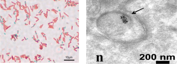
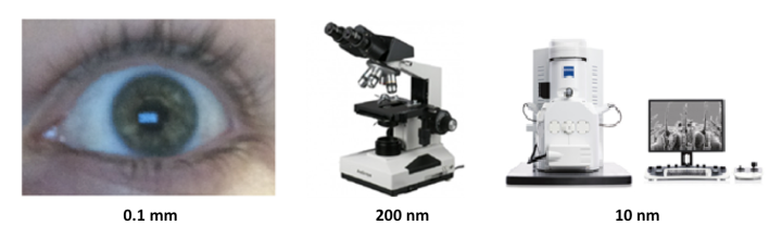
In order to be able to see things as small as nanoparticles, we need microscopes with very high resolution. As discussed in the blog post “What’s the difference between magnification and resolution?,” resolution is a measure of the shortest distance between two points that can be distinguished as separate regions by the observer. On the nanometer scale, traditional microscopy techniques cannot resolve the particles we need to observe. As a result, we turn to more powerful microscopy methods such as scanning electron microscopy (SEM) or transmission electron microscopy (TEM) to pierce the veil that cloaks the world of nanoparticles.
While compound microscopes use beams of light made up of photons in order to image objects, SEM and TEM use electron beams which allow them to resolve smaller objects. The key here is that electrons feature a higher frequency than photons, which allows a higher resolution to be obtained. To help picture this, we can use the metaphor of a ball bouncing across a floor that is covered by a blanket of fog. Whenever the ball hits the floor, it disperses the fog in that area, allowing you to see the spot on the floor where the ball landed. Although the electrons in an electron microscope aren’t pushing anything like the ball pushes the fog, this is a useful analogy because when a particle in the beam of a microscope hits a surface, we obtain information to “see” the area that it hit.
The ball analogy is also useful for understanding how frequency affects resolution in SEM and TEM. A ball that is bounced higher will contact the ground less often than a ball bounced lower because it takes more time for it to rise and fall—in other words, it has a lower frequency. The higher frequency ball will contact the ground more often, displacing more fog compared to the lower frequency ball. The larger number of collisions between the high frequency ball and the ground reveals more of the floor as a result. More of the floor being visible through the fog means a higher resolution image when using the high frequency ball compared to the low frequency ball.

So how does an SEM work? The high energy electron beam is produced by pulling electrons from a filament using either heat or an electric field, and then accelerating the electrons to a high energy.5 Once the electron beam contacts the sample, a large number of low energy secondary electrons are ejected from the sample surface and are accelerated towards a detector. The beam slowly moves back and forth along the sample and scans the whole sample area. (This movement, known as “rastering,” is what gives the technique its name.)
During the rastering process, a detector measures the amount of electrons being emitted from each region of the sample, and uses those measurements to construct an image. Regions with features closer to the detector have more ejected secondary electrons that reach the detector, corresponding to a lighter area in the constructed image. Conversely, the regions which feature valleys and divots are slightly farther from the detector, and will show up darker because fewer secondary electrons reach the detector from those areas. What you get in the end is a comprehensive image of the surface of your sample with a resolution up to about 10 nanometers. If you consider that atomic bonds are on the scale of a tenth of a nanometer (also called “angstroms”), this provides a fairly impressive picture!

TEM works similarly to SEM, except in TEM the detector is located beneath the sample rather than above it. This setup requires the electron beam to pass through (i.e. transmit through) a very thin sample. As the electron beam passes through the sample, some electrons hit atoms or electrons inside the material and scatter away from the detector. The rest of the electron beam makes it through to the detector, and creates what is essentially a shadow image of the sample. The advantage to this technique compared to SEM is a much higher resolution potential. The best TEM instruments can achieve sub-nanometer level resolution, and show individual atoms within a sample!
These two types of electron microscopy, SEM and TEM, have been used to resolve features as tiny as the features on the surface of pollen and even the patterns on the wings of butterflies (check out this post for more on that)!
We often use these specialized techniques in the CSN when we need to see objects on the nanometer scale. There are other techniques used for analyzing the atoms which make up these nanoparticles — more information on those techniques to come in a subsequent blog post. Stay tuned!
EDUCATIONAL RESOURCES
- ThermoFisher Scientific: An Introduction to Electron Microscopy
- Discovery Education: Virtual Electron Microscope
- AshaRani, P. et al. Cytotoxicity and Genotoxicity of Silver Nanoparticles in Human Cells, ACS Nano, 2009, 3, 279-290. DOI: 10.1021/nn800596w
- King, Paul. What is the highest resolution humans can distinguish? Eyewire [blog], 2013. Retrieved from: http://blog.eyewire.org/what-is-the-highest-resolution-humans-can-distinguish/
- Miami University of Ohio. What is resolution? [n.d.] Retrieved from: http://www.cas.miamioh.edu/mbiws/microscopes/resolution.html
- Vickerman, J. C.; Gilmore, I. S. Surface Analysis: The Principal Techniques, 2nd; Wiley: West Sussex, 2009. ISBN: 978-0-470-01764-7
- Seal Laboratories. How SEM Works. [n.d.] Retrieved from: http://www.seallabs.com/how-sem-works.html


Is the high energy electron beam produced in a similar way to those in cathode ray tube displays?
Thanks for the question! The post author replies, “Yes! The electron beams in both applications are produced in similar ways. There are a few different electron guns that can be used in electron microscopy, but a common option operates very similarly to a cathode ray tube electron gun.”